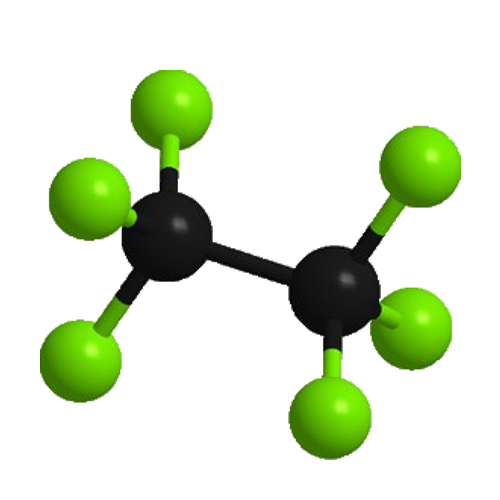
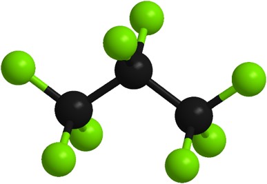
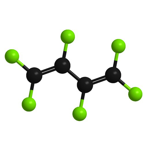
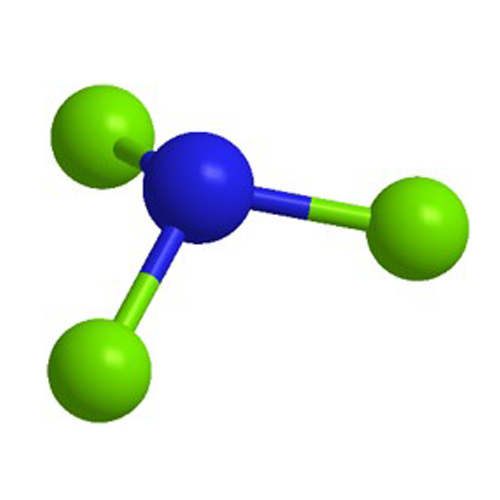
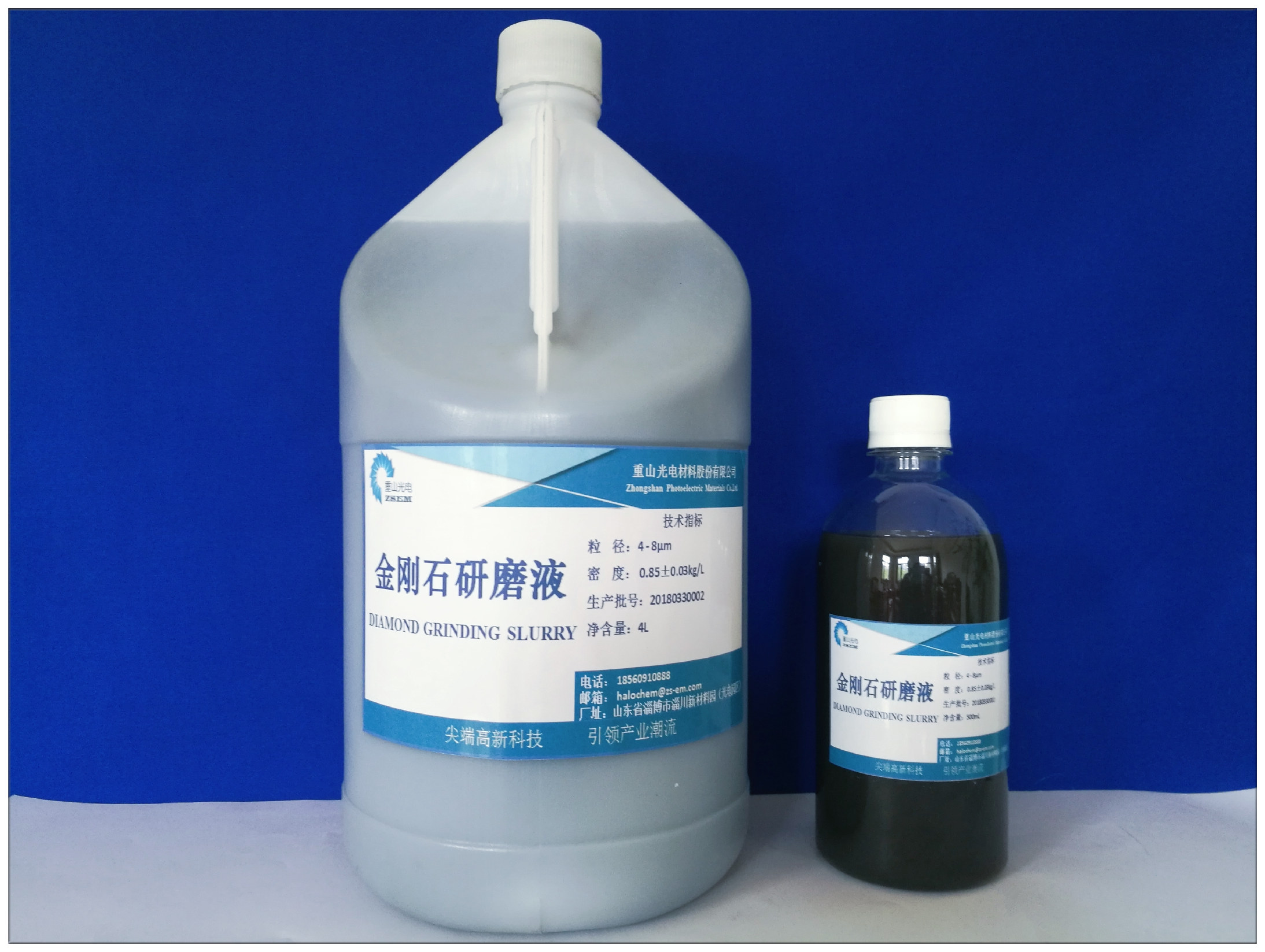
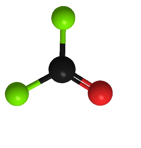
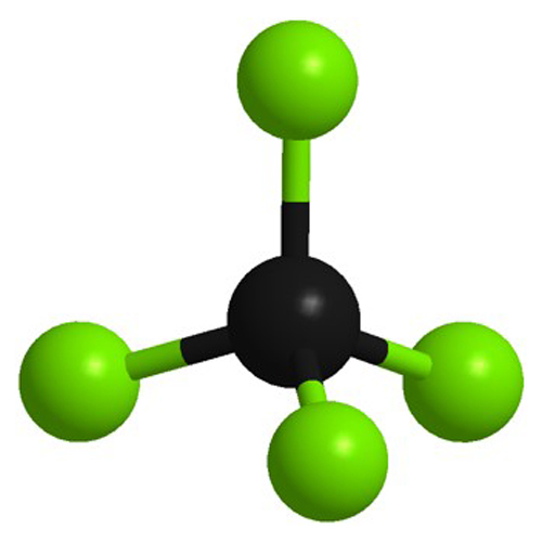
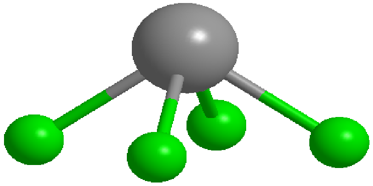
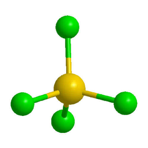
半导体工业的制造方法是在硅半导体上制造电子元件,而电子元件则由精密复杂的集成电路所组成,制作过程主要包括晶圆制备、晶圆制作IC(薄膜制作、微影制程、蚀刻、离子植入)、金属化制程、打线、封装与测试。半导体制程中,半导体材料主要为硅、锗、砷化镓等,微影制程中的光阻材料为感光剂、树脂和溶剂混合而成的感光材料,金属化制程主要用到绝缘材料和铝或铝铜合金,打线过程主要用到直径0.025mm左右的金线,最后用环氧树脂或陶瓷材料填入封装。在半导体制程中,集成电路的蚀刻是一个至关重要的过程。伴随着半导体工业技术的发展以及集成电路中的组件尺寸的精细化,等离子蚀刻技术因其可实现各向异性刻蚀、工艺兼容性好、刻蚀残存物少等优点,在半导体制程等得到越来越广泛的应用。本公司生产的半导体材料主要为三氟化氮、全氟丁二烯、六氟乙烷、八氟丙烷等氟化物蚀刻气体。
Semiconductor manufacturing is a process that the electronic component are manufactured on silicon semiconductor, while the electronic components are made up of sophisticated integrated circuit, the process mainly includes manufacture of wafer, manufacture of IC with wafer (manufacture of thin film, photolithography, etching and ion implantation), metallization process, wire bonding, packaging and test. There are some materials used in the process of semiconductor manufacturing, semiconductor materials mainly include silicon, germanium and gallium arsenide. Photoresist used in the photolithography is a kind of photosensitive material which is mixed with photosensitizer, resin and solvent. Insulating material, aluminium and albronze are used in the metallization process, gold thread with diameter of 0.025mm is used in the process of wire bonding. Finally epoxy resin and ceram material are used in the process of packaging. Plasma etching of integrated circuits is a crucial process in semiconductor manufacturing. With the development of semiconductor industry technology and the refinement of component in integrated circuits, plasma etching technology has been widely used in semiconductor manufacturing process due to its advantages such as anisotropic etching, process compatibility and few etching residues. The etching gas manufactured by our company is usually fluoride gas, including nitrogen trifluoride, perfluorobutadiene, hexafluoroethane, octafluoropropane, etc.